Where analog electronics deals with a limitless spectrum of voltage levels, digital electronics imposes strict boundaries. By categorizing voltage into distinct "high" and "low" bands, digital circuits achieve immense immunity to noise. This abstraction enables the execution of boolean mathematics, making it possible to construct processors, memory arrays, and hardware accelerators. This guide covers the mathematical theory, basic gate structures, and the timing constraints necessary to design reliable digital systems.
The Digital Abstraction
In a digital system, continuous voltages are discretized into two logic states, typically represented as Logic 1 (True) and Logic 0 (False). For instance, in a 3.3V CMOS system, any voltage above 2.0V might be interpreted as a logical 1, while any voltage below 0.8V is interpreted as a logical 0. The gap between these thresholds is the noise margin. If a signal falls into this undefined region, the logic gate's interpretation becomes unpredictable, leading to metastability and data corruption.
Boolean Algebra
Digital design relies on Boolean algebra, a branch of mathematics where variables can only hold the values true or false. Unlike standard algebra, operations in Boolean algebra are logical rather than arithmetic. The three fundamental operations are:
- Conjunction (AND): True only if all inputs are true.
- Disjunction (OR): True if at least one input is true.
- Negation (NOT): Inverts the input state.
Using theorems such as De Morgan's Laws, complex logical expressions can be simplified, minimizing the number of hardware gates required for physical implementation.
Combinational Logic
A combinational logic circuit is one whose output is solely determined by the current state of its inputs. There is no memory, no concept of past events, and no clock signal driving operations.
Fundamental Gates
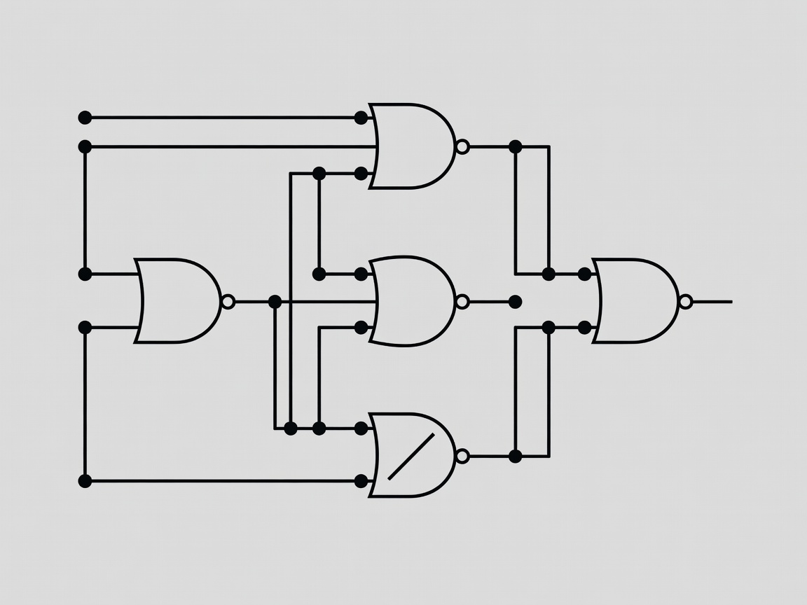
Transistors act as microscopic switches to construct logic gates. Beyond the basic AND, OR, and NOT gates, universal gates such as NAND and NOR are heavily utilized. They are "universal" because any logical function can be constructed using only NAND gates or only NOR gates, which dramatically simplifies the semiconductor manufacturing process.
Multiplexers and Decoders
Common combinational blocks include multiplexers (MUX) and decoders. A multiplexer takes multiple data inputs and uses a control signal to route one of them to a single output line. It acts as a digital switch. A decoder performs the inverse, taking a binary input code and activating one specific output line out of many, which is critical for memory addressing.
Sequential Logic and Memory
While combinational logic evaluates current inputs, sequential logic introduces the concept of memory. The output of a sequential circuit depends not only on the current inputs but also on the history of past inputs. This is achieved through feedback loops.
Latches vs. Flip-Flops
The basic memory element is the latch, typically constructed from cross-coupled NAND or NOR gates. Latches are level-sensitive, meaning their output can change continuously as long as the enable signal is asserted. This makes timing analysis difficult in complex systems.
To create predictable, synchronized systems, engineers use flip-flops. A D-type flip-flop captures the value of its input (D) only at a specific instant—the rising or falling edge of a clock signal—and holds that value steady at its output (Q) until the next clock edge. This edge-triggered behavior forms the basis of synchronous digital design.
Finite State Machines (FSM)
A Finite State Machine is a computational model used to design sequential logic circuits. An FSM consists of a set of states, a set of transitions between those states, and actions. They are categorized into two types based on how outputs are generated:
- Moore Machine: The outputs are determined strictly by the current state. This design is highly stable and immune to transient glitches on the inputs, but it typically requires more states to execute complex protocols.
- Mealy Machine: The outputs depend on both the current state and the current inputs. Mealy machines can respond to input changes within the same clock cycle, making them faster and requiring fewer states, but they risk passing input glitches directly to the output.
Timing and Propagation Delay
Logic gates are not instantaneous. The time it takes for a change in input to reflect at the output is called the propagation delay. In a synchronous circuit, data must travel through combinational logic and arrive at the next flip-flop with enough time to be captured securely before the next clock edge.
Two critical timing metrics apply to flip-flops:
- Setup Time (tsu): The minimum time data must remain stable before the clock edge arrives.
- Hold Time (th): The minimum time data must remain stable after the clock edge has passed.
Violating setup or hold times causes metastability, where the flip-flop output enters an undefined voltage level, ultimately leading to catastrophic system failure. Understanding these delays dictates the maximum clock frequency at which a processor or digital system can operate.