A schematic diagram verifies that a circuit is logically and electrically sound in theory, but a Printed Circuit Board (PCB) brings that design into the physical world. The layout process introduces parasitic elements—unintentional capacitance, inductance, and resistance—that can degrade high-speed signals or cause power supplies to oscillate. Successful PCB design requires a meticulous understanding of material properties, layer stackups, routing strategies, and manufacturing tolerances.
Schematic Capture and Footprints
The design process begins with schematic capture, where symbols representing electronic components are connected logically. This phase defines the "netlist," a database of every electrical connection in the circuit.
Crucially, every abstract schematic symbol must be associated with a precise physical footprint for the layout phase. Footprints define the copper pads, drill hole sizes, and physical boundaries of a component. A mismatch between the theoretical component and the physical footprint is a common source of costly manufacturing failures.
Layer Stackup Management
A modern PCB consists of alternating layers of conductive copper and insulating dielectric (typically FR-4 fiberglass). Designing the layer stack is the most important decision in layout planning.
- 2-Layer Boards: The simplest structure, featuring copper on the top and bottom. Signal routing competes with power and ground paths, making it difficult to maintain continuous return paths for high-frequency signals.
- 4-Layer Boards: The standard for modern digital design. A typical stackup utilizes the top and bottom layers for signal routing, while dedicating the two internal layers as solid continuous planes (one for Ground, one for Power). This dramatically reduces electromagnetic interference (EMI) and improves signal integrity.
- Multi-Layer Boards (6, 8, 12+): Used in dense designs, such as computer motherboards or high-speed networking gear, to provide multiple isolated routing layers and multiple ground planes for advanced impedance control.
Placement and Thermal Strategies
Before routing a single trace, component placement dictates the success of a layout. The placement phase prioritizes short connections for critical, high-speed, or high-current nets.
Thermal management also dictates placement. High-power components like switching regulators or motor drivers generate significant heat. A board designer must provide sufficient copper area—often using thermal vias to stitch heat down to internal ground planes—to dissipate this energy, preventing the silicon from exceeding its maximum operating junction temperature.
Routing and Signal Integrity
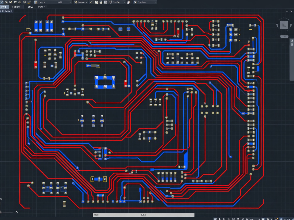
Routing is the process of drawing the physical copper traces that fulfill the netlist connections. Traces are not ideal wires; they act as transmission lines at high frequencies. When a signal transitions rapidly (fast edge rates), it behaves as an electromagnetic wave traveling along the trace.
Return Paths
Every electrical signal requires a return path to the source. For low-frequency signals, the return current takes the path of least resistance. For high-frequency signals, the return current takes the path of least *inductance*, which lies directly underneath the signal trace on the nearest continuous ground plane. If a trace crosses a gap in the ground plane, the return current must detour, creating a large loop area that radiates electromagnetic noise and compromises signal integrity.
Decoupling Capacitors
Digital ICs draw sudden spikes of current when millions of internal transistors switch simultaneously. The inductance of power traces limits how fast the main power supply can deliver this current, leading to voltage dips (ground bounce). Decoupling capacitors are placed immediately adjacent to the power pins of ICs, acting as tiny local energy reservoirs to supply these transient current demands without disrupting the broader power network.
Design for Manufacturing (DFM)
A perfectly routed board is useless if it cannot be fabricated. PCB manufacturers have specific physical limits known as design rules. These include minimum trace widths, minimum clearance between traces, and minimum drill sizes.
Engineers run automated Design Rule Checks (DRC) to ensure their layout complies with the manufacturer's capabilities. Once verified, the design is exported into standard manufacturing files (commonly the Gerber format), which contain the geometric data for the photolithography, drilling, and solder mask application processes necessary to physically construct the board.